ChipOnTime Technologies Pvt. Ltd. is a new-age semiconductor solutions company empowering innovation through cutting-edge design, development, and collaboration — bridging the gap between technology and talent to fast-track SoC development lifecycles.


Founded in 2019 and headquartered in Bangalore, India, ChipOnTime Technologies Pvt. Ltd. is an emerging semiconductor design and engineering solutions provider.
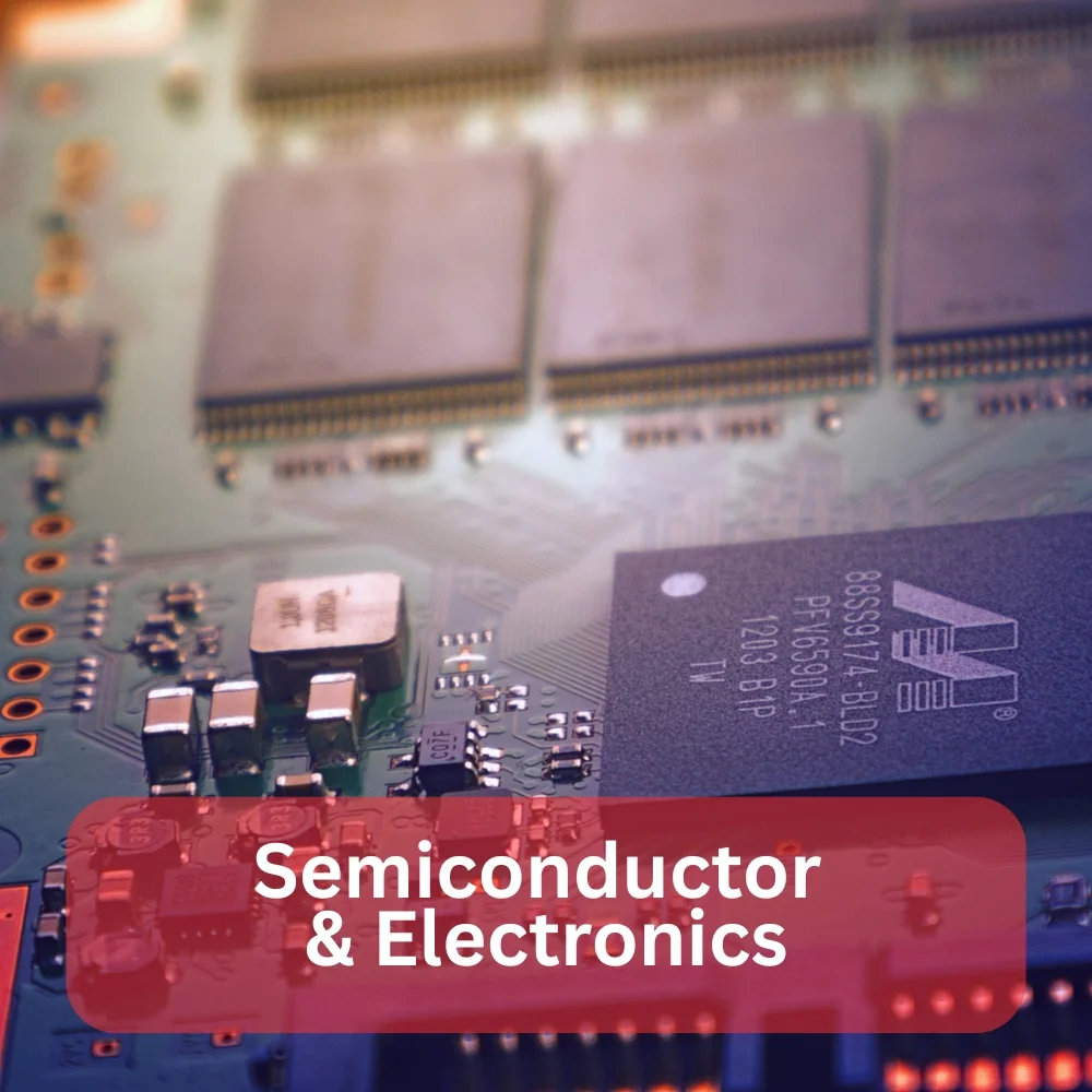
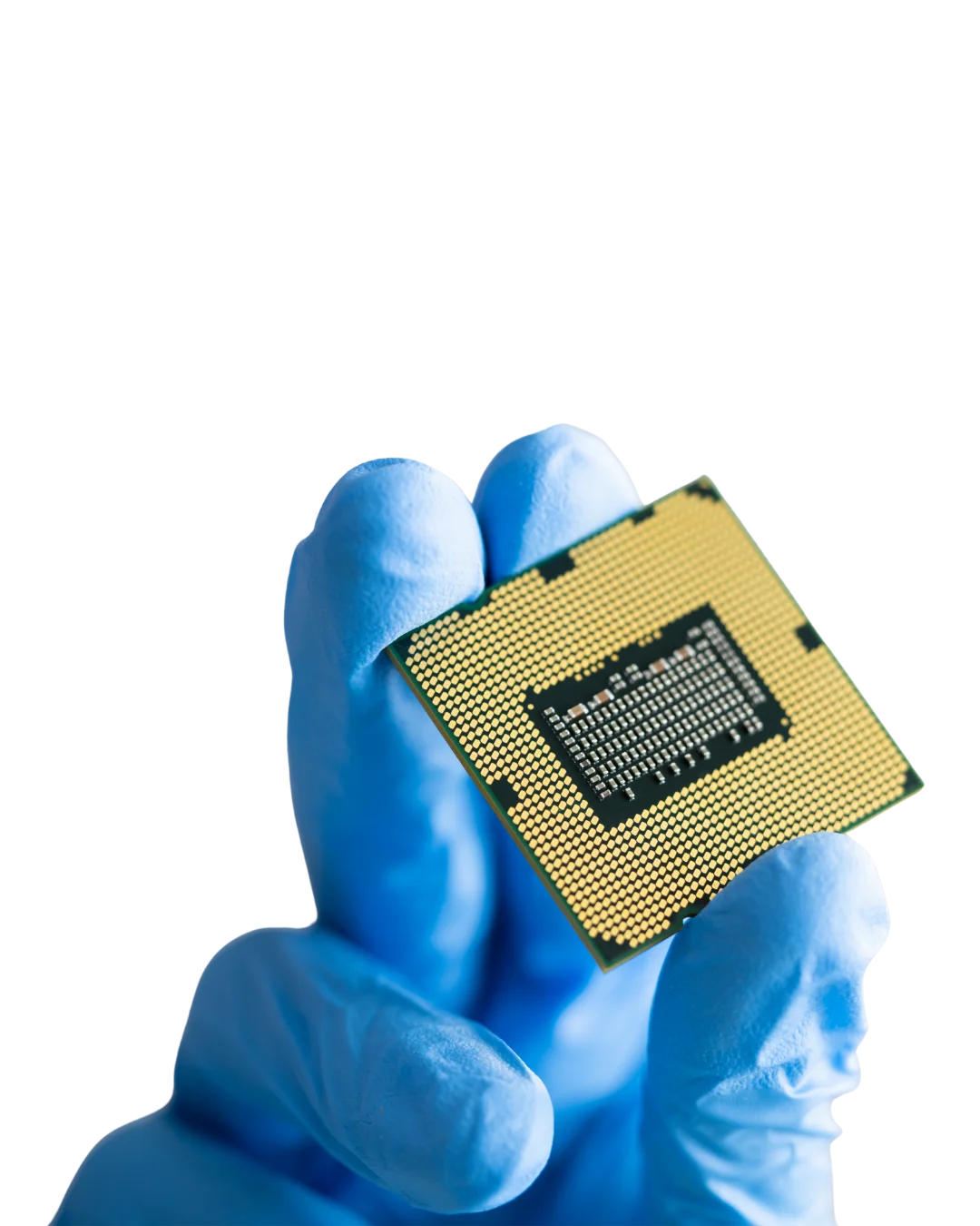
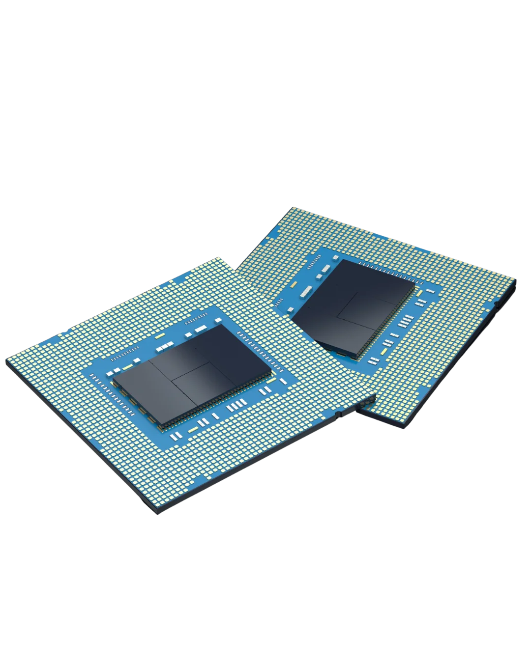
We specialize in end-to-end semiconductor design services, offering support across ASIC, SoC, DFT, PD, and verification domains.
Our goal is to accelerate Time-to-Market (TTM) for our clients through scalable, high-quality, and cost-effective engineering services.
With a foundation built by experienced semiconductor professionals, we take pride in delivering solutions that optimize Power, Performance, and Area (PPA) for every design.
To be a globally recognized partner delivering on-time, quality-driven semiconductor services that power the future of electronics.
To accelerate the semiconductor design lifecycle through innovation, collaboration, and excellence in engineering solutions.
Integrity: Honesty and transparency in every engagement.
Innovation: Consistent pursuit of technical excellence.
Collaboration: Empowering teamwork and collective growth.
Commitment: Delivering every project—on time, every time.
From RTL to GDSII, we cover the entire semiconductor design flow.
10+ years of combined industry experience across multiple global tapeouts
Proven expertise from 130nm down to 3nm technology nodes
Supporting clients in India, USA, Europe, China, Japan, Taiwan, Malaysia, and Singapore
Connecting skilled engineers with leading semiconductor companies to fill critical talent gaps
Focused on achieving the best Power, Performance, and Area metrics for every project
At ChipOnTime Technologies, we deliver comprehensive semiconductor design and engineering services — from ASIC and SoC development to verification, physical design, and analysis. Our expert team ensures precision, performance, and faster time-to-market across every stage of the chip design lifecycle.
From specification to implementation, we provide robust ASIC design support to ensure your chip meets the highest standards of performance and reliability.
Our experts deliver block-level and SoC-level verification using the latest simulation tools and testbench environments to ensure functional accuracy.
We perform detailed GLS to verify post-synthesis functionality and timing closure, ensuring production-ready silicon.
Optimizing designs for efficient test coverage and minimal overhead, our DFT engineers enhance yield and quality across projects.
From netlist to GDSII, our physical design team handles complex nodes and tapeouts with precision and scalability.
Ensuring timing integrity through comprehensive analysis and optimization to meet stringent performance goals.
We ensure power efficiency and performance stability by evaluating IR drop, electromigration, and thermal constraints.
We deliver precision-driven analog and RF layout design services tailored for advanced semiconductor nodes.
At ChipOnTime, we combine deep semiconductor expertise with a commitment to precision, collaboration, and timely delivery. Our experienced engineers, proven methodologies, and global exposure ensure every project meets the highest standards of quality, performance, and reliability — helping clients achieve faster time-to-market and long-term success.
Partner with ChipOnTime Technologies to accelerate your semiconductor design journey. From concept to silicon, our expert engineers ensure precision, performance, and on-time delivery — every step of the way.
We partner with companies across multiple sectors, delivering semiconductor and embedded design services for:


Their engineers bring real depth in physical design and verification. Truly a partner you can rely on
ChipOnTime has been instrumental in helping us close complex design challenges ahead of schedule. Their technical depth in Physical Design and STA, combined with a proactive communication approach, made our collaboration seamless and efficient.
What stands out with ChipOnTime is their consistency and engineering precision. The team understood our project requirements quickly and delivered outstanding results with minimal iterations. They’ve truly earned our trust as a reliable design partner.
Internship AIM : Empowering graduates with hands-on experience in Digital (CHIP)-Design. Our Training program bridges the gap between academics and industry, making them Job-ready and future proof.
Course Duration : 4 Months (16 Weeks)
Tools Used : Cadence Virtuoso & Genus


“Embracing technology & innovation, we stay ahead of the curve and shape the future”
From concept to completion our team delivers solutions that push boundaries and exceed expectations across every industry we serve.


We provide end-to-end semiconductor design services including ASIC Design, RTL Verification, DFT, Physical Design, STA, IR Drop Analysis, and Analog/RF Layout Design.
We serve clients across Semiconductor, Automotive, IoT, AI/ML, Medical Devices, Consumer Electronics, and Networking industries worldwide.
Our core expertise lies in Physical Design, RTL Verification, and Design for Testability (DFT), ensuring optimized Power, Performance, and Area (PPA) for every project.
We are headquartered in Bangalore, India, with plans to expand our operations to Hyderabad and Chennai soon.
Yes, we collaborate with global semiconductor leaders in India, the USA, Europe, China, Japan, Taiwan, Malaysia, and Singapore.
Our team has extensive experience working with nodes ranging from 130nm to 3nm, including Samsung and TSMC advanced process technologies.
We follow a proven delivery model emphasizing rigorous design validation, efficient communication, and milestone-based tracking to ensure every project is delivered on time and with precision.
Absolutely. We offer Turnkey, ODC (Offshore Design Center), and T&M (Time and Material) engagement models to suit specific client needs and project scales.
Yes, we believe in nurturing young talent and offer opportunities for fresh engineering graduates passionate about semiconductor design and verification.
You can reach us at info@chipontime.com or fill out the contact form on our website. Our team will get back to you promptly to discuss your requirements.

Our team is ready to assist you with expert support and quick answers for any challenge you are facing.

At ChipOnTime Technologies Pvt. Ltd., we’re always ready to collaborate, innovate, and deliver. Whether you need custom semiconductor design services, technical support, or partnership opportunities — our team is here to help you achieve faster Time-to-Market with precision.


ChipOnTime’s expertise and commitment to timely delivery helped us meet aggressive project schedules without compromising quality